
Every pad needs to be drilled with a 1mm bit so as to allow for components.
Resistors and Diodes are a great place to start with soldering. With the board face down, they rest flat and stay in place while soldering.

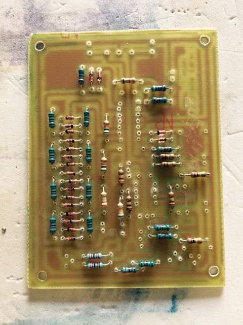
Bottom of board. I give the board a healthy layer of solder flux before going to work. I also solder over all the traces. It isn't necessary, but it prevents copper corrosion and sometimes I just like to see the solder flowing.

Awaiting three npn transistors to complete this board. Then on to the jacks and pots.

Device under test.


Calibration requires setting pot values full clockwise, and crimping a probe tip to pin one of IC 1A. Next a 1khz sine wave at input is compared to the wave shape at pin 1 of IC 1A. The trim pots on the pcb are then used to shape a symmetrical sine wave. Further trim adjustment is made to ensure that the unit is mute at 0v = envelope closed state.

Wave-forms before calibration. Bottom is the input reference sine-wave.
gLike
Wave Folder - Signal Processing Module
This circuit is a device which provides wonderful sonic possibilities. This module performs a non-linear transformation of a simple waveshape (triangle or sawtooth) into a complex waveform rich in overtones.
View Website