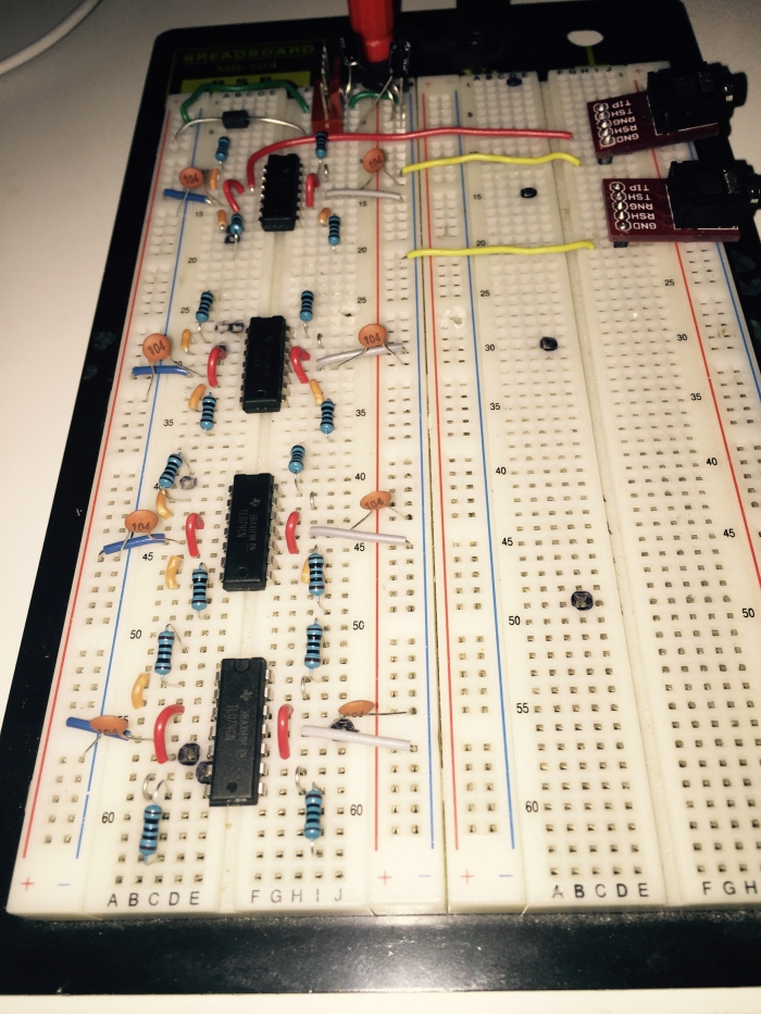
Initial breadboard build.
Initial test and debug. No issues, so it's time to move toward getting the circuit onto a PCB.
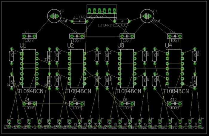
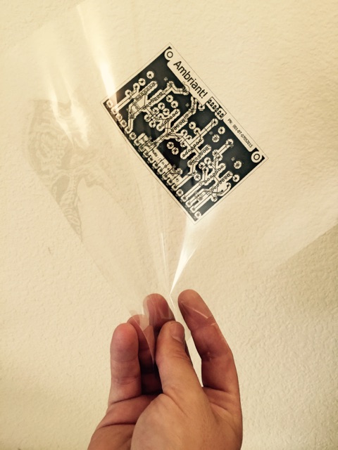
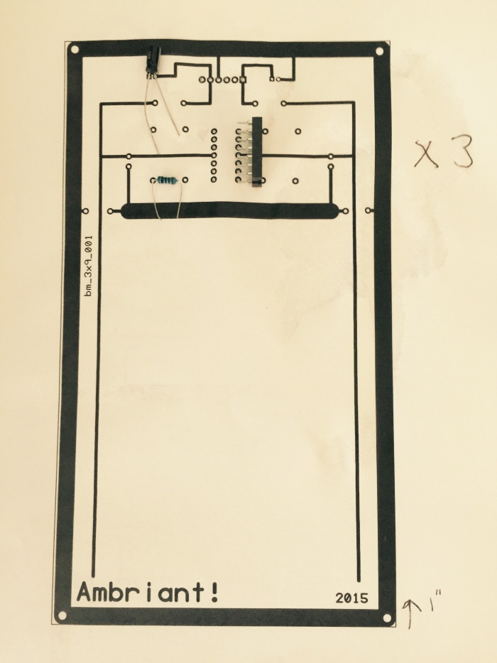
Printing out the CAD design to compare against actual component sizes is a worthwhile practice. A sheet of plain copy paper is cheaper than plowing through transparency sheets. This was also useful for making adjustments to hole sizes within my CAD design.
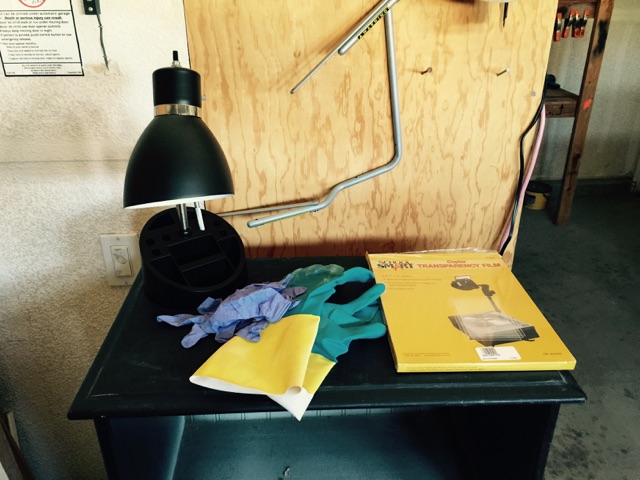
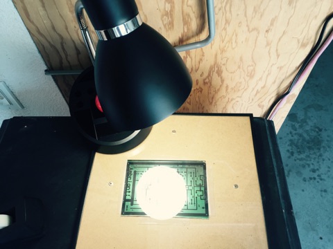
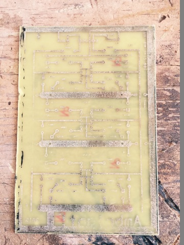
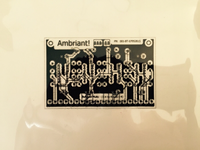
My first etch was a disaster. It turns out that I was using a standard lighbulb, which doesn't emit enough ultra violet light to properly expose the board. This resulted in a low contrast image, which ultimately resulted in copper traces which were shorted. The copper was too thin and being etched away. This was corrected by using a common CFC light bulb on the next exposure. This was a ten dollar mistake which I don't intend to repeat.
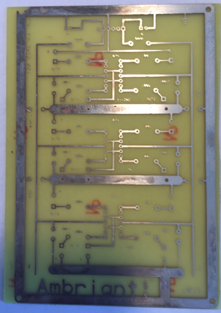
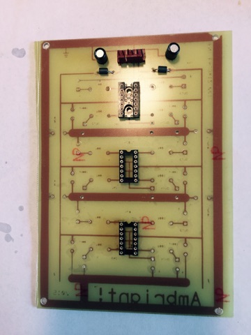
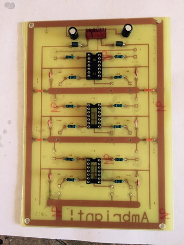
This time around I have nice dark copper traces. I have treated this board in a bath of liquid tin so as to prevent the copper from corrosion over time. I also like the way it looks.
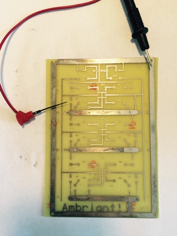
A continuity check on all the vias is a great way to build confidence in the signal traces before committing any components to solder.
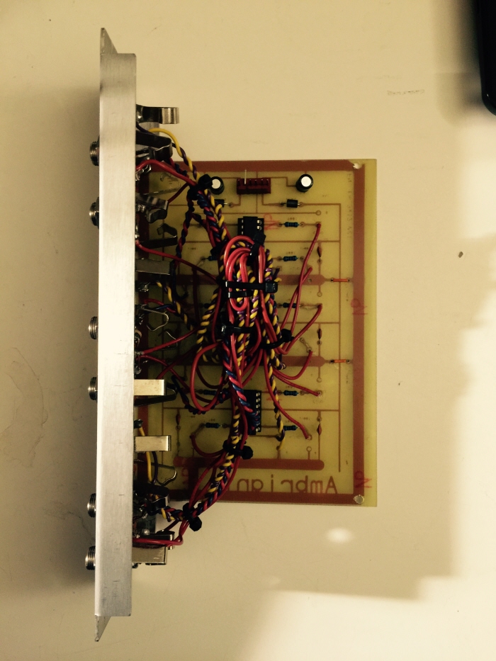
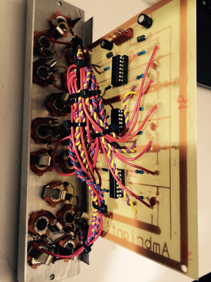
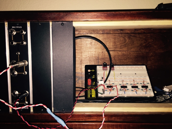
I always like to cable tie those twisted pairs so that they don't get snagged when removing from the case.
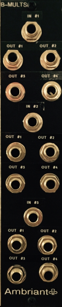
The board is exposed at the side of the module so one has to be careful when installing and removing the module. It's always best to power down the entire system first, just to be safe.
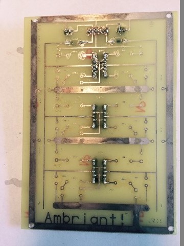
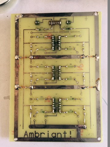
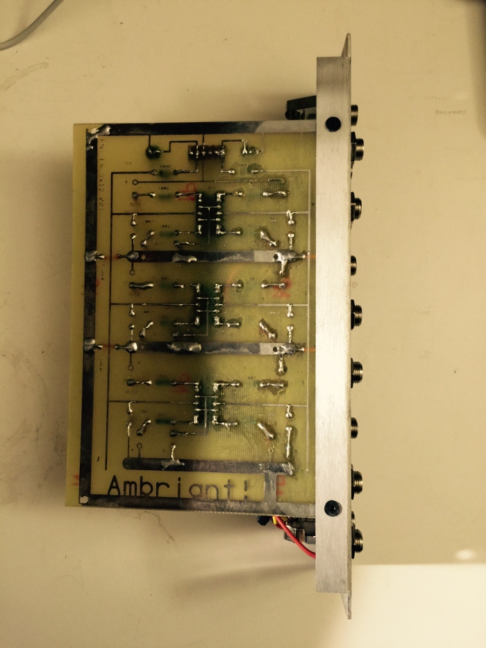
All together now. I have tested the unit and it meets expectation. No noise introduced and no anomalies with performance.
gLike
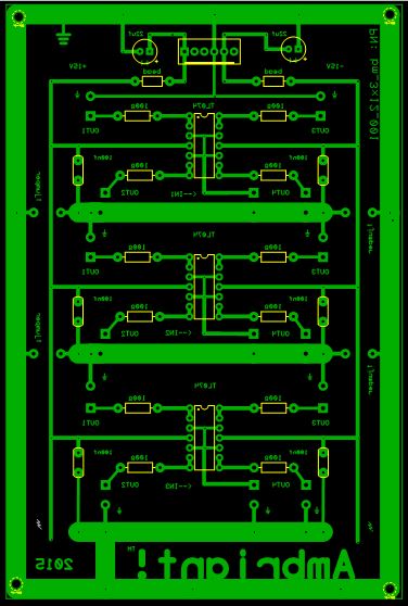
Buffered Multiples - Module
Status: In Progress
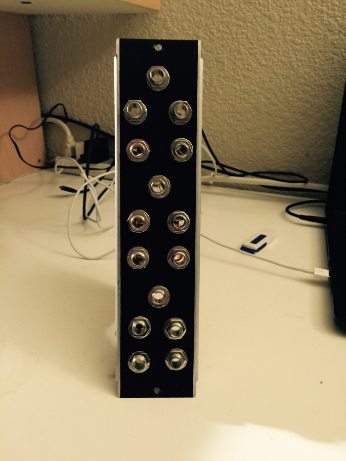
Buffered Multiples Module with 1 in to 4 outs x 3.
Features:
-Unity gain buffer
-DC coupled for use with CV or Audio signals.
-PCB CAD design
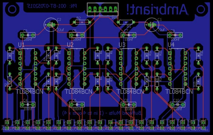
-Positive Resist Photo Etched PCB